Tuesday 25 April 2017

Lab power supply

My new power supply.

For quite some time I have been wanting an adjustable power supply. Both for convenience and hacker credits. Unfortunately, a really good one with all the goodies that I would like to have (multiple outputs, measurements, current limiting, computer control) is somewhere in the €4-to-500 range, which I find a bit too much.

But I still want my fancy power supply!! So I started thinking about making my own. Unfortunately I have no real experience with designing these things. Because of that it seemed a good idea to start with building some kind of kit. This would give me some experience, and possibly give me something to tinker with to see what works and what not.

After some browsing on the Internet I found this kit. It had favourable reviews, and a nice set of features: 0-28V, 0.01-2A, current limiting, short circuit protection,  digital display, current and voltage measurements, all for less than €20!

Of course, I needed to add some other stuff to make it a fully working PSU. A case, heat-sink, fan and banana plug terminals I found on eBay, and a mains switch, mains connector, knobs and a toroidal transformer I bought on-line.  A fuse holder, stand-offs and miscellaneous bits of wire and fasteners came from the well-known pile-of-stuff-that-I-might-need-in-the-future.

Assembling the actual kit was the most straightforward part of the exercise. All parts where there, all through-hole, so no worries at all. The design consists of two boards: an analog board that contains the rectifier, filters and power transistor, and a digital board that has an ATMEGA8, LCD, and two rotary encoders. A ribbon cable connects the two boards, and carries power, two voltage signals coming from the analog board that represent the output current and voltage, and one voltage signal going into the other direction that controls the power transistor. All regulation is done in software, so the ATMEGA monitors the output voltage and current, and adjusts the signal to the power transistor to maintain the correct output. The concept seems very similar to this.

The more involved part of the built actually was the mechanics. Getting a proper case for it, making the right holes in the case, and finding a way to mount everything safely and securely inside. The first case I bought turned out to be a bit too small, so I had to order a new one. As it turned out, that one was actually the same model as in the pictures of the seller of the kit.
First attempt at mounting stuff. In the end I added some stand-offs to the fuse-holder, so it no longer sits directly against the back panel. And I put a bit of anti-slip netting for the transformer to help it to stay put.

For mounting I tried to limit the number of holes in case, for looks, but also very much because any metal parts sticking through the case could potentially carry a large potential in the electrical sense. So I glued some stand-offs behind the front panel of the case to attach the digital board and display. To fix the transformer to the case, I stuck a metal bolt through the plastic lid (of a peanut butter jar), and glued that to the bottom. For glue I used two-component epoxy, which seemed to work reasonably well on the materials involved.

On the back of the case I added a mains connector, and a fuse holder on the inside. The fuse itself caused me some problems. I initially figured that a ~200mA slow fuse should be sufficient. Unfortunately, even 500mA fuses kept blowing during power-up, most likely because the large filter capacitor draws quite some current initially when charging. At the moment, I am using a 1A fuse, which should be good enough to prevent fire, but might not be good enough to prevent the transformer from getting damaged if ever the electronics fail catastrophically.
Everything on the inside. The digital board sits in front, the analog board on the left side, and the transformer on the right.The fan on the heat-sink is triggered by a temperature sensor, and draws air through in the bottom of the case. 

The power supply is able to deliver up to 2A at up to 28V, and can be used in voltage limiting or current limiting mode. It constantly shows the set maximum voltage and current, and what is currently actually delivered. The two rotary knobs change the voltage and current set-points, and pressing a knob stores the set-point as a default. The fan occasionally switches on (triggered by a temperature sensor on the heat-sink), but at least during my typical usage it is hardly ever  needed. So far I am very happy with the power supply. It is especially convenient to be able to see the output current when powering something.

As the ATMEGA8 had two unused pins, it should be possible, in principle, to add a serial interface for controlling it from a computer. This would involve moving some signals around to free up the UART pins, but that is hardly a problem.  Other things on my wish list would be a output enable/disable switch, a mode where the supply switches off when exceeding the current or voltage set-point, and set/used power  (in Watts) on the display, next to current and voltage. I think most of this could be implemented in software, but I would have to start from scratch. Unfortunately, the AVR came already programmed, and the flash memory was locked, so I could not download the software for hacking. I decided to leave these possible improvements for another day,

Anyhow, at the moment I am more than happy enough with the supply as it is. So for now I will spent my time on other projects.


Another view from the top.

Sunday 16 April 2017

Resurrection of a Lenovo Ideapad K1: to neon or not to neon

In my previous post here I discussed my struggle with flashing my wife’s Lenovo Ideapad K1. And in the end I had to conclude that I could not conclude that I have bad flash or bad memory. This all was interesting, but not so helpful to get the tablet back to usable again.

When I install my images:
  • First: CM10.1_Wifi_Kaschemme_v1 or K1_CM10_JB_Starter_v2 with the nvflash tool.
  • Second: cm-10.1.3-RELEASE-k1-wifi.zip or cm-10.1-20130916-NIGHTLY-k1.zip with the recovery firmware CWM6.0.x.x.
I don't have any problems. The problems start after installing the gapps that are missing in these CyanogenMod android 4.1 / 4.2 images.  I use for that the file gapps-jb-20130427-nonneon-tonyp-keyboard.zip

I did a bit more research on my problems. There are a few elements to my "not working" tablet which helped me to narrow down the issue:
  • Messages that various google services have stopped or are not working any more.
  • Programs like youtube that not start or google play that gives [RH01] errors.
  • Logfile that gets filled with SIGILL errors and register dumps.
The last symptom  helped me most. After some time spend with google search I started to understand that I am hitting here an essential Tegra 2 vs Android 3.2+ issue.

The Tegra 2 T20 was at the time a relative advanced dual core Cortex A9 processor with a very good GPU so that it could do video decoding and encoding in the GPU. The Arm part is good but the GPU was the more advanced Nvidia item. A bit similar situation like the BCM2835 SoC processor of the Raspberry pi. Only is this not an ARMv6 but real ARMv7-A architecture, but to reduce some costs/complexity they have not implemented all the typical Cortex-A9 functions like the Advanced SIMD (NEON) extension. Probably Nvidia expected not to need this because the GPU could do the multimedia power lifting much better. From Tegra 3 Nvidia starts to support the full "instruction set".

The SIGILL error happens when a program is trying to execute a NEON instruction on a not NEON processor.  In the past, older than Android 4.1, was the assumption that most processors were ARMv5 and did programs not use NEON instructions, also not for AMRv7A.  In the SDK was it also explicitly asked for to have libraries for ARMv5 and ARMv7A with and without NEON or other extensions.

The issue I now have in 2017 looks to be two fold:
  • Google started to ship APK packages optimized for NEON, maybe on purpose, maybe by accident or maybe the compiler starts to optimize more/better in this direction.
  • For higher android versions is NEON compatibility of the ARMv7A architecture assumed.
This means that when a newer Android is installed on a tegra 2 platform we will hit the lack of NEON support. The program or parts of it will crash when there are no backup libraries for NEON emulation. All the google service packages and programs such as the google play, youtube etc. have this (potential) problem. My issue is that this "newer" is already by the Android 4.2 from the CM10 images and that the gapps package is pulling in a lot of newer versions of the libraries to support certain API's to talk back to Google and the Android universe.

It must be possible to keep and skip to the correct versions of the google apps to keep them working. However that is not so easy. There is always the danger that a new installed app is bringing the system down.

At this moment I see as only option to stay at android 3.2 and not to update too much. I have installed the old not rooted official Lenovo image: K1_A301_11_11_111108_US.zip and with that older outdated version is for the last hours youtube and the web browser working.

Case closed: a working tablet with obsolete Android 3.2 and an odd ball ARM device in my collection.

A side note: this tablet went obsolete in early 2012 and therefore there are still some people working on it up to late 2013. There are quite some messages in the XDA and Lenove forums from that time, but nowadays are all links in the posts to file sharing servers dead. It is very difficult to find various images back. Therefore it is not really possible to have a long life on this kind devices in terms of (software) support. The PC is in that way a much durable concept.

Short update: Improved Android 3.2.1 image

I searched a bit longer and found here the following thread with a better Android 3.2.1. image for this tablet. This image has the following improvements:
  • Newer version of the root file system: 14_14_120109 build
  • Recovery image / bootloader
  • No levono market and other not working apps
  • Rooted
The original image name is: K1_Stock_120109_nvflash_R2.zip but it can also be found as honeycomb.zip

Saturday 15 April 2017

Resurrection of a Lenovo Ideapad K1

My wife is the lucky owner of an Lenovo Ideapad K1, an Android 10" tablet I have bought for her in 2011.  Lenovo is clearly not supporting the product any more; an  difficult findable product on their own website.  This was a relative cool product, tegra 2 based and 1GB memory and 32 GB flash, that I could buy at the time in Japan. This tabled was a nice toy to consume media like reading websites of watching youtube movies.
However a few years back I got all kind of strange problems; programs crashed, the tablet didn't boot / come out of sleep  mode, etc.  Flashing a newer CyanogenMod firmware helped only for some time.
Recently I have taken the dust of the tablet to have a deeper look into the problems I am experiencing with the thing.

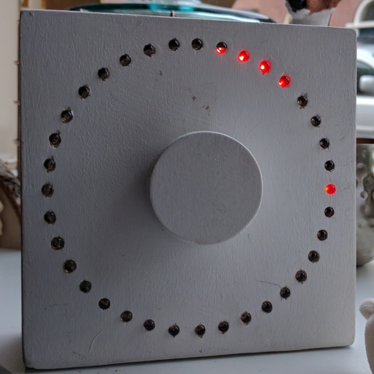
Lenovo IdeaPad K1 with crashes and errors in log file (CatLog)


Most information can be found in the XDA forums; this posting is a good start to find the required files.
I mainly used:
  • Recovery / first file system: nvflash_CM10.1_Wifi_Kaschemme_v1.zip
  • Main CyanogenMod firmware file system: cm-10.1-20130916-NIGHTLY-k1.zip and/or cm-10.1.3-RELEASE-k1-wifi.zip
  • Google apps items: gapps-jb-20130427-nonneon-tonyp-keyboard.zip

Detailed information

The following (among more) is inside:
  • An Nvidia Tegra 2 T20 processor at 1GHz.
  • The flash chip is Toshiba 32 GbB emmc chip with a now way obsolete 2nd generation controller in a painful to (de)solder BGA package: 32GB Toshiba THGBM2G8D8FBA1B NAND Flash.
  • The memory chip is also a BGA package: 1GB Eplida B8132B2PB-6D-F LPDDR2 DRAM.
Changing things in the hardware will be very hard and/or impossible.

The device has the following partition table:
Partition number Name Start sector Num Sectors Size Mbyte Description FS type Android / Linux mount point
2 BCT 0 1024 4 System configuration data data
3 PT 1024 512 2 Partition table data
4 EBT 1536 1024 4 Bootloader ? data
5 GP1 2560 512 2 also some bootloader related partition table data
6 SOS 3072 1536 6 Recovery partition android boot /dev/block/mmcblk0p1
7 LNX 4608 2048 8 kernel /boot partition android boot /dev/block/mmcblk0p2
8 APP 6656 107520 420 System root partition ext4 /dev/block/mmcblk0p3
/system
9 CAC 114176 32768 128 Cache partition ext4 /dev/block/mmcblk0p4
/cache
10 MSC 146944 512 2 miscellaneous data /dev/block/mmcblk0p5
11 USP 147456 35840 140 Bootloader ? data /dev/block/mmcblk0p6
12 UDA 183296 6740992 26332 User data ext3 /dev/block/mmcblk0p7
/data
13 TMP 6924288 614400 2400 Temp partition ext4 /dev/block/mmcblk0p8
14 GPT 7538688 276480 1080 Partition table data

The hope is that I can identify

Contacting the boot loader

One of the important steps is to get "contact" with the bootloader to get a deeper understanding of the state of the flash.
The tegra has a possibility to boot over USB. That means that the ROM bootloader is not getting its further data from flash (nand, sd, emmc), but waits on data coming from the USB subsystem. This is a special protocol of Nvidia.

The linux tool for this is called nvflash, this program can be found in the archive of the upgrade images. More information can be found here or with google.

The first step in the process is to get a more "advanced" bootloader working on the process so that actually communication and flashing is possible. For this is a special "Nv3p server" bootloader needed (bootloader.bin).  Because of the secure system should this bootloader  be accompanied by a key in a binary blob (blob.bin).  And there is the need for a kind of board description file BCT file (flash.bct) to let the bootloader know what kind of memory and flash is used. This all can be found in the flash package for android.


Making an udev rule

By making an udev rule is it possible to set the correct permissions and to remove the need to be root to communicate with the tablet. This is actually linux basics, but not something I do daily so I personally forget all the details every time.

Basic work flow:
Check location of the device with lsusb:
$ lsusb
Bus 003 Device 012: ID 0955:7820 NVidia Corp. Tegra 2 AC100 developer mode

Check the relevant parameters for the udev script:
$ udevadm info -a -p $(udevadm info -q path -n /dev/bus/usb/003/012)
  looking at device '/devices/pci0000:00/0000:00:14.0/usb3/3-3/3-3.1':
    KERNEL=="3-3.1"
    SUBSYSTEM=="usb"
    DRIVER=="usb"

    ATTR{idProduct}=="7820"
    ATTR{idVendor}=="0955"
    ATTR{ltm_capable}=="no"
    ATTR{manufacturer}=="NVIDIA Corp."
    ATTR{maxchild}=="0"

Make the udev rule:

$cat /etc/udev/rules.d/60-nvflash.rules 
# nvflash support for Nvidia Tegra systems attached to USB
SUBSYSTEM=="usb", ATTR{idVendor}=="0955", ATTR{idProduct}=="7820", MODE="0660", GROUP="plugdev"

Reload the rules and check if something is recognized:

$ sudo udevadm control --reload-rules 
$ udevadm test /devices/pci0000:00/0000:00:14.0/usb3/3-3/3-3.1
$ sudo udevadm monitor 

Getting data from the flash chip


With the following commands is it possible to get the partition table and the data of each partition. The first command ensures that the Nv3p server is up and running.

$ ./nvflash --blob blob.bin --bct flash.bct --odmdata 0x300c0011 --bl bootloader.bin --getpartitiontable partition.txt
$ ./nvflash --resume read 12 UDA.bin
$ ./nvflash --resume read 3 PT.bin

This did not result into an error. So reading from flash does work in principle. Next is a sanity check of each partition, where the data partitions are most important.

$ file UDA.bin
UDA.bin: Linux rev 1.0 ext3 filesystem data, UUID=1d1ae925-25c3-4daf-a78c-5e92106cad73 (large files)
$ fsck.ext3 -v -f UDA.bin
$ mkdir -p test
$ sudo mount UDA.bin test

Here are errors found. I am not certain if this means we have errors on our flash chip or that the file system just crashed by a hard shutdown before.

Re-flashing the device

I try to flash the image with the verify option switched on.

$ ./nvflash --blob blob.bin --bct flash.bct --odmdata 0x300c0011 --configfile flash.cfg --bl bootloader.bin --format_partition 2 --sync
$ ./nvflash -r --format_partition 2
$ ./nvflash -r --format_partition 3
          ....
$ ./nvflash -r --format_partition 14
$ ./nvflash -r --blob blob.bin --bct flash.bct --setbct --odmdata 0x300c0011 --configfile flash.cfg --create --verifypart -1
Nvflash v1.8.90246 started
[resume mode]
Using blob v1.1.57813
sending file: flash.bct
- 4080/4080 bytes sent
flash.bct sent successfully
odm data: 0x300c0011
setting device: 2 3
creating partition: BCT
creating partition: PT
creating partition: EBT
creating partition: GP1
creating partition: SOS
creating partition: LNX
creating partition: APP
creating partition: CAC
creating partition: MSC
creating partition: USP
creating partition: UDA
creating partition: TMP
creating partition: GPT
Formatting partition 2 BCT please wait.. done!
Formatting partition 3 PT please wait.. done!
Formatting partition 4 EBT please wait.. done!
Formatting partition 5 GP1 please wait.. done!
Formatting partition 6 SOS please wait.. done!
Formatting partition 7 LNX please wait.. done!
Formatting partition 8 APP please wait.. done!
Formatting partition 9 CAC please wait.. done!
Formatting partition 10 MSC please wait.. done!
Formatting partition 11 USP please wait.. done!
Formatting partition 12 UDA please wait.. done!
Formatting partition 13 TMP please wait.. done!
Formatting partition 14 GPT please wait.. done!
done!
Enabling verification for partition ID = 4...
sending file: bootloader.bin
\ 1393296/1393296 bytes sent
bootloader.bin sent successfully
Enabling verification for partition ID = 6...
sending file: recovery.img
\ 4573184/4573184 bytes sent
recovery.img sent successfully
Enabling verification for partition ID = 7...
sending file: boot.img
| 2816000/2816000 bytes sent
boot.img sent successfully
Enabling verification for partition ID = 8...
sending file: system.img
- 264010336/264010336 bytes sent
system.img sent successfully
Enabling verification for partition ID = 13...
sending file: userdata.img
And for some reason is the process hanging at this point. The userdata.img file is smaller than the system.img file; I would expect that the flash process goes with the same speed or faster. Is this than the sign that flash or memory is bad? The tablet feels warm so maybe it is from calculating the checksum; I will have to wait for an hour.
Waiting is not really working. When the verification option is enabled is the userdata.img always failing around 139657210 bytes. This does not become better when I move partition 13 a significant amount of sectors forward. Probably this means I have a memory problem and not a flash problem.
A normal write, without the checksum calculation for the verify, does work normally.

$ ./nvflash --bl bootloader.bin --blob blob.bin --bct flash.bct --setbct --odmdata 0x300c0011 --configfile flash.cfg --create 
Nvflash v1.8.90246 started
Using blob v1.1.57813
rcm version 0X20001
System Information:
   chip name: t20
   chip id: 0x20 major: 1 minor: 4
   chip sku: 0x8
   chip uid: 0x0428914840c12157
   macrovision: disabled
   hdcp: enabled
   sbk burned: true
   dk burned: true
   boot device: emmc
   operating mode: 4
   device config strap: 0
   device config fuse: 0
   sdram config strap: 0

sending file: flash.bct
- 4080/4080 bytes sent
flash.bct sent successfully
odm data: 0x300c0011
downloading bootloader -- load address: 0x108000 entry point: 0x108000
sending file: bootloader.bin
\ 1393296/1393296 bytes sent
bootloader.bin sent successfully
waiting for bootloader to initialize
bootloader downloaded successfully
setting device: 2 3
creating partition: BCT
creating partition: PT
creating partition: EBT
creating partition: GP1
creating partition: SOS
creating partition: LNX
creating partition: APP
creating partition: CAC
creating partition: MSC
creating partition: USP
creating partition: UDA
creating partition: TMP
creating partition: GPT
Formatting partition 2 BCT please wait.. done!
Formatting partition 3 PT please wait.. done!
Formatting partition 4 EBT please wait.. done!
Formatting partition 5 GP1 please wait.. done!
Formatting partition 6 SOS please wait.. done!
Formatting partition 7 LNX please wait.. done!
Formatting partition 8 APP please wait.. done!
Formatting partition 9 CAC please wait.. done!
Formatting partition 10 MSC please wait.. done!
Formatting partition 11 USP please wait.. done!
Formatting partition 12 UDA please wait.. done!
Formatting partition 13 TMP please wait.. done!
Formatting partition 14 GPT please wait.. done!
done!
sending file: bootloader.bin
\ 1393296/1393296 bytes sent
bootloader.bin sent successfully
sending file: recovery.img
\ 4573184/4573184 bytes sent
recovery.img sent successfully
sending file: boot.img
| 2816000/2816000 bytes sent
boot.img sent successfully
sending file: system.img
- 264010336/264010336 bytes sent
system.img sent successfully
sending file: userdata.img
- 142382496/142382496 bytes sent
userdata.img sent successfully
This probably means that I will have to search for a memtest tool for the tegra.
The tool to check the sdram didn't work for me. Nvidia has some special tools but they are not free available or ask for a special memory description files.  I can maybe get those out of the bct file but still...
The output below is what the nvflash tool is giving me:

$ ./nvflash --cmdhelp --odm
Nvflash v1.8.90246 started
--odm command usage ->
nvflash --odm CMD data --bl  --go
-----------------------------------------------------------------------
used to do some special diagnostics like sdram validation, fuelgauge etc
each CMD has data associated with it
For e.g.
1. SD/SE diagnostic tests:
   nvflash --odm runsediag  --bl  --go
   nvflash --odm runsddiag  --bl  --go
   ---------------------------------------------------------------------
   used to run SD/SE diagnostic tests, where N is the input parameter like
   SDController Instance.
2. Sdram verification:
   nvflash --bct  --setbct --configile  --create --odmdata     --odm verifysdram  --bl  --go
   ---------------------------------------------------------------------
   used to verify sdram initialization i.e. verify sdram params in bct is
   in accordance with actual SDRAM attached in device or not.
   N can be either 0 or 1. '0' implies soft test where known word patterns
   are written for each mb and read back. This word pattern validates all
   the bits of the word. '1' implies stress test where known word patterns
   are written on entire sdram area available and read back. This tests every
   bit of the the entire available sdram area
-----------------------------------------------------------------------
$ ./nvflash -r --bct flash.bct --configfile flash.cfg --odmdata 0x300c0011 --odm verifysdram 0 
Nvflash v1.8.90246 started
[resume mode]
command failure: no commands found

Conclusion

I cannot really conclude that my memory or flash is bad, despite of the "struggle" I had with the nvflash tool. In general I don't see errors with the flash process, and when I have an error then they don't depend on the flash location and are probably more a not related "feature" of the nvflash tool and bootloader firmware.
A memory error would be still possible, but in that case I would have expected more often problems and real hard crashes.
The conclusion must be that I have a different problem.

Saturday 25 March 2017

Odroid U3 and the emmc memory

Introduction

The Odroid U3 board can, just as all other Odroid boards, use eMMC memory instead of a micro SD card. This type of memory is not only more "cool" but also much faster.  When I bought my board I did order a 8 Gb eMMC module with Ubuntu on it. My recent thinking was to put Openelec on the eMMC instead of the Ubuntu that came with the board.
Back side Odroid U3 with eMMC (red dot) installed, Micro SD card and eMMC adapter


I have downloaded an image from the Odroid forum here.
With the normal procedure I copied the image to the eMMC:

gunzip OpenELEC-Odroid-U2-6.0.1.0.img.gz
sudo dd if=OpenELEC-Odroid-U2-6.0.1.0.img of=/dev/sdh bs=1M
sync
sudo umount /dev/sdh1
sudo umount /dev/sdh2

All good and booting the board with the eMMC and the following messages from uboot:

OK
U-Boot 2010.12-svn (May 12 2014 - 15:05:46) for Exynox4412
CPU: S5PC220 [Samsung SOC on SMP Platform Base on ARM CortexA9]
APLL = 1000MHz, MPLL = 880MHz
DRAM:  2 GiB
PMIC VERSION : 0x00, CHIP REV : 3
TrustZone Enabled BSP
BL1 version: 20121128
Checking Boot Mode ... EMMC4.41here
REVISION: 2.0
Manufacture ID 0x11 [ 7456MB ] 
NAME: S5P_MSHC4
MMC Device 0: 7456 MB
MMC Device 1: 0 MB
MMC Device 2 not found
*** Warning - using default environment
USB3503 NINT = OUTPUT LOW!
ModeKey Check... run normal_boot 
No ethernet found.
Hit any key to stop autoboot:  1
do_fat_cfgload : cmd = fatload mmc 0:1 0x41000000 boot.ini
reading boot.ini
2697 bytes read in 21 ms (125 KiB/s)
Find boot.ini file. But This file is not odroid4412 config file!
NAME: S5P_MSHC4
NAME: S5P_MSHC4
>>> Load Boot Script from mmc 0:1 <<<
reading boot.scr
** Unable to read file boot.scr **
>>> Load Boot Script from mmc 0:2 <<<
** Unrecognized filesystem type **
>>> Run Default Bootcmd <<<
reading kernel..device 0 Start 2455, Count 16384 
MMC read: dev # 0, block # 2455, count 16384 ... 16384 blocks read: OK
completed
reading RFS..device 0 Count 18839, Start 2048 
MMC read: dev # 0, block # 18839, count 2048 ... 2048 blocks read: OK
completed
Wrong Image Format for bootm command
That didn't work. The same procedure with a micro SD card did result in a booting system.

Somehow is something going wrong with u-boot.
Working micro SD version:
Odroid # version

U-Boot 2015.10 (Feb 29 2016 - 22:54:24 +0000)
armv7a-openelec-linux-gnueabi-gcc-4.9.3 (GCC) 4.9.3
GNU ld (GNU Binutils) 2.25.1
Not work eMMC version from the same image:
Exynos4412 # version


U-Boot 2010.12-svn (May 12 2014 - 15:05:46) for Exynox4412
How can that be, two different versions of u-boot from the same image file?

The old U-boot of 2010.12 is not compatible with the boot.ini file and probably also not with the kernel format / identifier of what ever. It is clearly necessary to use the U-Boot 2015.10 version.

Difference between SD and eMMC


The reason is that the Exynos4412 Prime soc is intended for secure operation. That means that the bootloader and software has to be signed and that a couple of further "hidden" security features are used when an eMMC is available instead of an SD card.
This results in a complicated booting process:
  1. ROM
    The rom loader starts when processor is powered up / has had a hard reset. Based on hardware settings (boot pins and availability of interfaces) is the next step boot loader put in to the L2 cache memory
  2. BL1
    The signed bootloader "BL1.bin" is pulled into the SOC this is a binary blob that comes from Samsung. It is signed with a key / encrypted. This loader fits into the L2 cache is is able to configure the memory of the processor so that the next boot loader actually fits into the memory.
  3. BL2 +  TrustZone
    This loader is basically a signed part of U-boot. This U-boot part is signed by the key of Hardkernel and is therefore an acceptable payload for the BL1 loader.  At this point is also the "TrustZone" configured a kind of security level in the processor to enable things like DRM and payments. From this point U-boot can be loaded.
  4. U-Boot
    This is the normal opensource boot loader that understands eMMC, SD, USB, network and the file systems. This loader puls the kernel into the memory and will start it.
  5. Kernel and initrd
    When this part is loaded and started we have at last a working linux system.
The different boot loader parts are differently stored on the SD card and unfortunately not in the same way on the eMMC card.

The different blocks are on the SD or eMMC as follows organized:
Binary Block offset Part type
name SD eMMC (eMMC only)
Bl1.bin 1 0 1 (boot)
Bl2.bin 31 30 1 (boot)
U-boot.bin 63 62 1 (boot)
Tzsw.bin 2111 2110 1 (boot)
Uboot Env 2500 2500 0 (user)

What stands out s that the eMMC uses a boot/secure part for the bootloader. This part can (normally) not be accessed from the operating system or when the eMMC is used as SD card. This done to be able to guarantee a secure system and to have a un-brick-able configuration. The user cannot change the bootloader and therefore not really brick the board. Only with a special u-boot or a special kernel module is it possible to access the secure partition.

Basically this means that the boot loader is not updated when an image is written to the eMMC card in it's sd adaptor.

How to update u-boot on an eMMC

Hardkernel has an eMMC recovery tool available. This is an image with a special u-boot that updates the secure boot partition of the eMMC with new bootl loaders. This tool can be found on their forum here. I have used image exynos4412_emmc_recovery_from_sd_20140629.zip, but as always your mileage may vary.

This image must be written to an SD card as normal. The procedure is as mentioned on the Odroid forum as follows:
  1. Prepare a microSD card and flash the attached image.
  2. Boot with the microSD without eMMC
  3. Turn on U2/U3 and wait for a few seconds and blue LED will blink.
  4. Plug your eMMC module into U2/U3
  5. Plug micro-USB cable into U2/U3 and connect other side to your PC USB host or ODROID's USB host port. (This is a trigger to start the recovery)
  6. After recovery process (only a few seconds), the blue LED will turn off automatically.
  7. Finish. Install OS on your eMMC with as usual.
When we look at the SD with the image we see the following structure:

hansan@Desk-computer:~$ ls -l /media/hansan/48E0-7CDF/*
-rw-r--r-- 1 hansan hansan 2701 Jun 28  2014 /media/hansan/48E0-7CDF/boot.ini

/media/hansan/48E0-7CDF/update:
total 662
-rw-r--r-- 1 hansan hansan  15360 Mär 18 12:37 bl1.bin
-rw-r--r-- 1 hansan hansan  14592 Mär 18 12:37 bl2.bin
-rw-r--r-- 1 hansan hansan   1392 Jun 28  2014 sd_fusing.sh
-rw-r--r-- 1 hansan hansan 159744 Mär 18 12:37 tzsw.bin
-rw-r--r-- 1 hansan hansan 478121 Mär 18 12:37 u-boot.bin
-rw-r--r-- 1 hansan hansan   2105 Mär 18 12:37 update.sh
hansan@Desk-computer:~$ 

This means that the special u-boot on the SD card is pulling the boot loader parts from the update directory and put those files into the secure boot partition of the eMMC. To make openelec working on an eMMC is it necessary to put the new U-Boot 2015.10 into the boot partition of the eMMC. This can be done by first extracting the boot loader parts for openelec and copy them to a recovery image. That image updates the boot partition and after that is it possible to write the openelec image to the eMMC. This results in a working combination.

My approach to get to the correct version of u-boot was to compile openelec from source.  A different approach would be extracting the parts of the SD-card and save them under the correct names.

I have downloaded the source from here. And followed the instructions:

1. Unpack sources
2. make PROJECT=Odroid DEVICE=$DEVICE image
3. wait for compilation.
4. zcat target/OpenELEC-Odroid-$DEVICE-6.0.2.0.img.gz | dd of=/dev/mmcblk0

    $DEVICE can currently be either U2, XU3 or C1

5. SD card is now complete.
I did need to mangle the download site for the "liberation-fonts-ttf" package. Google on the error messages received during complication can help to fix the issues.  The required files can be found in the image directory.

hansan@Desk-computer:$ ls ./build.OpenELEC-Odroid.U2.arm-6.0.2/image/system/usr/share/bootloader/
bl1  bl2  tzsw  u-boot  update.sh
These four files have to be copied to the SD card with the eMMC recovery image update directory. Don't forget to add the .bin extension to match the "pattern" on the SD card.
With this image is it possible to update the u-boot on the eMMC module to the version need to boot the openelec image from eMMC. It is then not longer needed to use a SD card.
This new image can be backed up  to a file.

hansan@Desk-computer:$ sudo dd if=/dev/sdh of=~/work/Arm_sbc/odroid/openelec/eMMC_openelec_6.0.2.0.img bs=512 count=220501
220501+0 records in
220501+0 records out
112896512 bytes (113 MB, 108 MiB) copied, 6,31194 s, 17,9 MB/s
hansan@Desk-computer:$ 
I have put the updated recovery image here.

By the way it would also be possible to extract the required files from the Odroid OpenElec SD card image. That would remove the need/trouble of compiling the boot loader.


Saturday 18 March 2017

Fixing the SmartTV

Over the years I have collected a couple of ARM based boards evaluation / experimentation . Some I bought because just I wanted to and others I have bought for a specific purpose that they never fore filled.

I got recently so disappointed with the "SmartTV" part of my Samsung television UE40ES6300. The issues are that the applications are not very convenient (e.g. difficult to search in Youtube), the SmartHub always needs an update when it is inconvenient and in June 2016 was the support for Skype discontinued. The discontinuation of Skype would be enough for a own post.

The combination bad SmartTV, no Skype and Arm board gave me the thought that it would be maybe a solution to install AndroidTV on one of my boards. Such that I can enjoy a more stable experience, have a good working Youtube and Skype again because this all works so nice on my android telephone.

My board of choice for this is an Odroid U3 of Hardkernel.
Odroid U3

This is a board based on a Samsung Exynos4412 processor a quad core Cortex-A9 on 1.7GHz and with 2Gb of memory. Quite a potent processor that is also used for some of Samsugs galaxy telephones and tablets. This processor was discontinued / succeded with a newer version sometime Q2 2014.

I first tried Android TV CM 12.1 which did not do the trick for me.
  • The google play store did not work properly
  • Did not get used to the user interface, (More my problem)
  • To have skype support in your android device you need a "key" which is not available for this device / android combination.
The above made that this did not solve my requirements. With having to give up on Skype there was  no need to use Android. The next step would be a linux based media player (i.e Openelec with Kodi).

Openelec is also available for the Odroid U3 and can be found here on the Odroid forum. This worked for me better than Android, because of my better knowledge of linux. It is for me easier to understand what is happening under the hood than with Android. With Android I am more the stupid user than the "hacker" that can fix the internals.

I do have a couple of issues for which I will make a few blog entries:
  1. The image works very well from an SD card but not from the faster / sexier eMMC memory. The solution of that can be found here.
  2. My above mentioned television is not always detecting the HDMI and CEC interface, depending on who was switched on first. I will need to further look into this.
  3. It would be nice to only supply power to the board when the television is on. But this should not give a corrupt file system when the TV is switched off.


Wednesday 4 January 2017

Children's countdown timer

Occasionally, our children need some help with the concept of time. According to them, some of those minutes are much shorter than others (think watching TV vs. driving to the Efteling). To help them with this, I have been promising to make something for the past half year. But now it is ready!

After spending about two days on it over a period of six months, here is the result: a children's countdown timer. It shows clearly how much time is left for a certain activity, and also plays a tune when time is up.

The children's timer. Unfortunately, the multiplexing of the leds combines unfavourably with the shutter of the camera. To the naked eye, all leds in the upper-right quadrant are lit.

By turning the knob clockwise, more and more of the leds along the ring are switched on. After not moving the knob for 5 seconds, the timer starts counting down. One after another, the leds slowly decrease in intensity and switch off. Each led takes 100 seconds, so the full circle uses a full hour. When all leds are off, time is up and a song is played on a piezo buzzer while the leds show a flashy pattern. By turning the knob clockwise past "zero", it is possible to switch between silent mode and audible alarm (non-silent) mode. In non-silent mode, the buzzer also clicks when turning the knob, providing feedback on whether an audible alarm is enabled.

Under the hood

The main parts of the timer are 36 red leds, two 1.5V AA batteries, a 3.3V step-up converter from the parts bin (Sparkfun NCP1400-based), a rotary encoder (from conrad.nl), a piezo buzzer that came with an old computer mainboard, and an Atmel ATtiny2313 for a brain.
A look under the hood. The piezo buzzer, the step-up converter and the AVR are approximately on a straight line from the bottom-left to the centre. All leds are on, and the batteries deliver a current of 6.3mA.
The 36 leds are driven as 3 sets of 12 via charlieplexing, using 12 microcontroller pins. This arrangement uses more pins than multiplexing the leds in a single set, but it allows three leds to be lit at the same time, increasing the average brightness using less current. Without going into details, this has to do with the non-linear response of led vs. current.

Since debugging this kind of setup is very hard, I tried to keep the software as simple as possible. A single "master" timer fires an interrupt 2600 times per second. The main purpose of this is to refresh the "display". The correct leds are switched on or off according to what needs displaying. Four levels of intensity per led, 12 leds, and 2600 interrupts per second lead to a refresh frequency of 55 Hz, which shows no flicker (to the naked eye at least ;-)).


A look at the back side of the board. The other side can be so clean because this one is a bit of a mess.
After updating the display, the routine samples the two input pins connected to the rotary encoder. By filtering over 16 samples, the signals are debounced to get a reliable input. And finally, a software counter divides the master clock to generate a timer "tick" at 5 Hz to be used by the rest of the software for time-keeping.

Events for timer "ticks" and changes of the rotary encoder are communicated to the rest of the software using bit flags. After every interrupt, the main software loop wakes up, and if there is an event, this is handled in the loop.

To play music, a separate timer is connected to the piezo speaker, that generates the notes. The music is stored encoded in the flash image and played at a pace determined by the "tick" events ultimately derived from the master timer.

When the countdown timer is switched off, the oscillators of the microcontroller are disabled and the ATtiny enters a deep sleep mode. Just before this happens, one of the inputs connected to the rotary encoder is set-up such that it will wake up the microcontroller when the signal changes. If the rotary encoder is in a position where one of its inputs bounces between on and off, this could prevent the microcontroller from entering deep sleep. To counter this, the input that wakes the micro is alternated between the two inputs every time sleep mode is enabled. So if the AVR wakes up due to a bouncing pin, it will time out since there is no actual input after the debouncing filter. It then switches to the non-bouncing pin, and enters sleep mode again.

The software is written in C using avr-libc, and compiled by avr-gcc. The current version takes 1748 bytes of flash memory, leaving exactly 300 bytes for possible extensions. The circuit has a header that is compatible with an USBasp to allow in-circuit updating of the software, something that has already proved very useful. Since the circuit normally runs at 3.3V, but the USBasp needs 5V, it is necessary to disconnect the battery before programming, and power the circuit from the programmer itself. In hindsight, I should have added a jumper to make this more convenient and less error-prone, but so far I remembered to remove the batteries when needed.

I put the software on https://github.com/bart-h/avr-timer for those that are curious.

Power usage

Because the contraption runs of a battery, power usage is an important consideration. When switched off, the system itself draws an idle current of 0.5μA after the step-up converter. Assuming a battery capacity of 1Ah, this would correspond to a battery-life of 228 years! Or actually, it means that other things will dominate the battery drain. Before the step-up converter, about 12μA is used, mainly by the converter itself. Initially I was irked to fix this 4% efficiency problem, but then I realised that the battery life would still be 9.5 years. Close enough to infinity for my purposes.  And when the system is fully active, the efficiency increases to about 90%.

When the countdown timer is running and all leds are switched on, the system draws 6.3mA at the battery. Running a countdown of a full hour (starting with all leds on, and ending with all leds off) then uses 3.15mAh. Again assuming a 1Ah battery capacity, this would allow 317 runs, more or less one per day for a full year.

The largest power drain is by the buzzer and its series resistor. When it is driven high, it draws ~30mA. Fortunately, when playing notes, the buzzer is switched on and off constantly, as sound is made by voltage changes, not stable levels. This already halves the average current. In addition, the music contains pauses that set the buzzer to 0V. Because I do not have an integrating power meter, I do not know how much power is actually used when playing music. But because the tune takes no more than 20 seconds, I assume the power usage can be neglected in the overall scheme of things. While turning the knob, the buzzer also toggles to make clicking sounds. Here I took care to switch the buzzer level back to 0V as soon as possible, to conserve power.

Because an real Alkaline AA battery actually has a capacity closer to 2Ah, all calculated lifetime numbers should be doubled as well in reality. But the final proof will be when I have to replace the batteries...


The timer running when it is dark. Because the camera uses a much larger exposure time, all leds that are lit also appear on in the picture.