Sunday 10 November 2019

Upgrading an Eee PC 901


Our oldest daughter has many dreams. One of them is to make computer games. Being a techie myself, I feel I have to encourage such dreams. As a start I bought her a book to learn to program in Python. But to do this she needs access to a computer as well. As it happens I still own an old ASUS Eee PC 901 netbook. To me it is no longer very useful, but it would be perfect for my daughter.

So I took a good look at the machine. The keyboard and screen were still good. The battery was good enough, but one trackpad button was broken. And even when running Lubuntu it felt very slow. To make her first "own" computer experience a good one, I figured I should try to improve it. So I decided to fix the trackpad button, and invest about €20 on upgrades. Given the age of the netbook, it did not make sense to spent more on it.

An easy upgrade was maxing out the ram by replacing the 1 Gb DIMM by a 2 Gb one (8 euro delivered).

Performance of the built-in SSD. Note that this is the 4GB one. Its 8GB sibbling is even slower.
The next bottleneck of the system was the 12GB of flash storage, in the shape of a 4GB and a 8GB module. From what I could gather, this was implemented as some kind of compact flash internals on an PCI-express form-factor, via a PATA bus. Note that the PCI-express form-factor means that it is mechanically like PCI-express, but NOT electrically. All in all, this made for a very slow pair of SSDs that were also expensive to extend or replace.

Fortunately, the SSD connector also had a SATA interface hiding on it. And I already had bought a little PCB to break this out many years before, when I was still planning to use the system myself. So I went to AliExpress, and bought a cheap (13 euro shipped!) Netac 60Gb SSD. To make it fit in the system, I had to remove the case of the SSD and the SATA connector. This meant I had to solder the whole thing directly to the break-out PCB, but that was only a minor problem.

SSD soldered onto the break-out PCB.


Break-out PCB with SSD connected to the mainboard. Unfortunately, there was no 5V on the break-out PCB, so I had to take that from somewhere else.


To make this work even better, I flashed a new "3rd party" BIOS that enabled the AHCI SATA interface, as the stock BIOS only allowed the IDE compatibility mode. Unfortunately, this still did not allow me to boot from the SATA SSD, so I had to keep one original flash module to boot from. But as this is really only used to load the linux kernel and initramfs, that has very limited impact on performance.
New SSD is recognized by the BIOS!
Nice speed improvement!
Apart from the above, I also had to do two small repairs: one was to replace one of the above-mentioned buttons of the trackpad, as that was not working well anymore. The other was to bodge my SATA break-out PCB, as I managed to damage it when I tried to remove a connector.
Bodge needed because I damaged the tracks.


Another bodge to connect the replacement trackpad button.
Anyway, after these improvements, this system has another couple of years left in useful life!


22-6-2020: fixed spelling mistake.

Using the AVR USI to create a I2C peripheral device

As part of a more complex project, I recently felt the need to implement an I2C peripheral on an ATtiny2313, using its Universal Serial Interface ("USI"). As described in the link, the I2C protocol allows multiple devices to communicate using only two signalling wires.

In case you want to do something similar, here are a few suggestions that helped me a lot:
First of all, make sure that you can see what is going on. The main tools I used for creating and debugging were my DS1054 oscilloscope to look at the various signals, a Bus Pirate that can act as an I2C controller, and an USB-to-serial convertor connected to the AVR UART so that I could watch debug-messages.

And secondly, while I am generally very impressed with the quality of the AVR datasheets, the USI part was described a bit too loose for me to understand exactly what behaviour the various register settings would cause. So after some frustrating attempts, I started to dump the various USI-related registers over my serial debug output, to see what exactly happened. This helped to clarify some points, so I get my I2C peripheral to work.

Now to continue with the main story...

As said, the I2C protocol uses 2 signal-lines: SCL and SDA, being the clock and data line, respectively. Both of these are normally pulled high externally, and the devices on the bus pull them low (to ground) to communicate. Typically, the bus has one  controller device and one or more peripheral devices, but multiple controllers are possible as well.

During normal communications, SDA may only change when SCL is low. The two exceptions are the "start" and "stop" conditions. (The latter is only really important for controller devices, so I will not discuss it here.) Another important aspect of the protocol is that the controller controls the SCL line, but after the controller pulls the SCL low, peripheral devices are allowed to keep it low to slow things down in case they cannot keep up.


I2C protocol in a nutshell. Shown are the start condition ("S"), data transfer ("Bx") and stop condition ("P"). Original drawing by  Marcin Floryan and taken from wikipedia.


The "start condition" signal pulls SDA down when SCL is high. This acts as sort of a bus-reset, and makes all peripheral devices pay attention to what is coming next. Next step after pulling SDA down is that the controller also pulls the SCL down, to prepare for the first data-bit (remember that SDA normally only changes if SCL is low). Luckily, the AVR's USI helps us here. It can generate an interrupt when the SDA line goes low while SCL is high, and after the controller then pulls SCL low, the USI will keep it low until we tell it otherwise. This makes sure that even our slow code and a very fast controller will be in sync at a certain moment.

After the start condition, the controller will proceed by sending a string of 7 address bits, and 1 R/W (read-write) bit. The address bits identify for which peripheral the rest of the message is meant, and the R/W bit tells whether the controller expects to send or receive data. To read these 8 bits, we could simply setup the USI to sample a bit of SDA each time that SCL goes from low to high, do that for 8 bits, and then interrupt. But the way the USI works is that it counts in terms of SCL flanks (both low-to-high transitions, when a bit is sampled, and high-to-low transitions, that I will come to later), so we need 16 of those. Since high-to-low changes are counted as well, things get slightly more complicated, as explained below.

When serving the "start" interrupt, SCL might not have gone down yet, so we need to synchronise somewhere. All code I could find simple used a busy-loop to wait until the SCL went down. But busy-loops in interrupt routines is never a really good idea, especially when waiting for some external signal that is not under our control. So I did something more elegant: when the SCL line was still up, I set the USI to wait for one additional flank. Using the fact that the USI will keep the SCL low until released, and doing things in the right order, I could make this safe for race conditions. Unfortunately, the USI can only count a maximum of 16 flanks, and this scheme would need up to 17. So the next trick is to only sample the first 7 address bits, and count either 14 or 15 flanks.

ISR(USI_START_vect,ISR_BLOCK)
{
  /* Start condition.
   * Controller might still have to clock up at this point
   * Once it goes down, USI will keep it down, as long as we did not clear 
   * the start condition.
   */

  /* make sure that sda is in the right mode, as a start condition can happen
   * virtually anytime.
   */
  set_sda_input();
  set_sda_high();
  
  /* Next will be the 7 address bits (14 flanks on clock) */

  /* To prepare for the next step after receiving address, we need to "output"
   * 1s, so put those in the DR.
   */
  USIDR = 0xff;
  
  /* Assume clock is still high, so we prepare for 15 flanks, and fix it later. */
  set_status_register(0,1,15);

  /* Enable full mode */
  set_control_register(1,1,1);

  /* Setup for receiving address */
  i2c_peri_state = I2C_ADDRESS;

  /* Check if clock is down */
  if ((I2C_PIN & _BV(I2C_CLK))==0) {
    /* Line went down already, so only 14 flanks are needed now. 
     * Doing check like this will prevent racing.
     */
    /* Set 14 flanks.
     */
    set_status_register(0,1,14);
  }
  release_start_condition();
}
The code above shows how the "start" condition interrupt routine is done. Note that the release_start_condition() call is from where on the USI will no longer keep the SCL low after the controller pulled it down. More code and details can be found on my github.

Once the 7 address bits are received, we can check if we are the peripheral that is being addressed. If not, we can simply go off the bus, and wait for the next "start condition" signal. But if the address is correct, we need to get the R/W bit, and after that acknowledge our reception to the controller. In general, acknowledgement is done by the receiver after every 8 bits, by pulling SDA down for the 9th bit. As we already know that we should acknowledge, we can setup the USI to receive one more bit,  then pull SDA low (output a 0), for one more SCL cycle, and then interrupt again. By smartly combining the R/W bit and the acknowledge bit in 4 SCL flanks, we do this part with only three interrupts (start condition, first 7 bits, R/W bit and acknowledge). This is the same number of interrupts that other implementations use, because these need to handle the acknowledge bit separately as well.
/*
 * Overflow function: (some) data was transferred.
 */
ISR(USI_OVERFLOW_vect,ISR_BLOCK)
{
  uint8_t data;
  
  data = USIDR;
  if (i2c_peri_state & I2C_WAIT_ACK1) {
    /* We send a byte. Now try to get an acknowledge. */
    if (i2c_peri_state & I2C_WAIT_ACK2) {
      i2c_peri_state &= ~I2C_WAIT_ACK2;
      set_sda_input();
      set_status_register( 0, 1, 2 );
      goto go_leave;
    } else {
      /* check if the controller acked */
      if (data & 1) {
         /* NACK */
         goto go_idle;
      } else {
         i2c_peri_state &= ~I2C_WAIT_ACK;
         set_sda_output();
      }
    }
  } else if (i2c_peri_state & I2C_ACK_RECEIVE) {
    /* Done acknowledging our reception */
    i2c_peri_state &= ~I2C_ACK_RECEIVE;
    if (i2c_peri_state == I2C_IDLE) {
      goto go_idle;
    }
    /* release sda and set to input */
    set_sda_high();
    set_sda_input();
    /* wait for 16 flanks */
    set_status_register( 0, 1, 16 );
    goto go_leave;
  }
  
  switch( i2c_peri_state ) {
  case I2C_ADDRESS:
    /* First 7 address bits are received. */
    if (data==(0x80|(I2C_PERI_ADDR>>1))) {
      /* The address, now get our send-receive bit */
      i2c_peri_state = I2C_READ_WRITE;
      /* As this is our address, we can have the hardware do the acknowledge. */

      /* Enable output. 
       * This is okay, as the start ISR made sure that we are outputing "1", i.e. nothing.
       */
      set_sda_output();
      /* Clock is down. 
       * Next clock up will shift RW bit into DR0, and 0 to DR7
       * Next clock down will latch DR7 into SDA. -> ACK
       * Next clock up will shift our 0 into DR0, and 1 out to DR7
       * Next clock down will latch DR7 into SDA, i.e. release SDA again.
       */
      USIDR = 0xbf;
      /* Wait for 4 flanks. */
      set_status_register( 0, 1, 4 );
      goto go_leave;
    }
    /* not us, get off the bus */
    goto go_idle;
    break;
  case I2C_READ_WRITE:
    /* This is the tail end of the address phase.
     * Only the RW bit was still needed, and the ACK was
     * already dealt with by the hardware.
     */
    /* RW bit is the second bit */
    if (data&2) {
      /* controller requests data */
      i2c_peri_state = I2C_SEND_1;
      // we are ready to send now
      goto go_send;
    } else {
      /* controller will send more */
      set_sda_input();
      i2c_peri_state = I2C_CONTROL;
      /* prepare to receive 8 bits */
      set_status_register(0,1,16);
      goto go_leave;
      return;
    }
    break;
  case I2C_CONTROL:
    /* get our control value */
    i2c_peri_cmd = data;
    switch(data) {
    case 0x01: /* set pwm colors */
      i2c_peri_state = I2C_RECEIVE_6;
      goto go_ack_receive;
      break;
    case 0x10: /* read voltage */
      i2c_peri_state = I2C_IDLE;
      event_trigger( EVENT_I2C_PERI_CMD );
      goto go_ack_receive;
      break;
    case 0x20: /* read string */
      i2c_peri_send_buffer[0] = 0xde;
      i2c_peri_send_buffer[1] = 0xad;
      i2c_peri_send_buffer[2] = 0xbe;
      i2c_peri_send_buffer[3] = 0xef;
      i2c_peri_send_buffer[4] = 0xcc;
      i2c_peri_send_buffer[5] = 0xaa;
      goto go_ack_receive;
    default:
      goto go_idle;
    }
    break;
  case I2C_RECEIVE_1 ... I2C_RECEIVE_6:
    i2c_peri_receive_buffer[ i2c_peri_state - I2C_RECEIVE_1 ] = data;
    if (i2c_peri_masterstate == I2C_RECEIVE_1) {
      /* got all our bytes */
      event_trigger( EVENT_I2C_PERI_CMD );
      i2c_peri_state = I2C_IDLE;
    } else {
      --i2c_peri_state;
    }
    goto go_ack_receive;
    break;
  case I2C_SEND_1 ... I2C_SEND_MAX:
  go_send:
    // here we start sending...
    
    USIDR = i2c_peri_send_buffer[ i2c_peri_state - I2C_SEND_1 ];
    set_status_register( 0, 1, 16 );

    if (i2c_peri_state == sizeof(i2c_peri_send_buffer) ) {
      i2c_peri_state = I2C_IDLE; /* wait for ack, and go idle */
    } else {
      ++i2c_peri_state;
    }
    /* Setup so we wait for an ACK afterwards */
    i2c_peri_state |= I2C_WAIT_ACK;
    goto go_leave;
    break;
    
  case I2C_IDLE:
  default:
    goto go_idle;
  }

 go_idle:
  i2c_peri_go_idle();
 go_leave:
  return;

 go_ack_receive:
  /* we need to acknowledge our receiving... */
  i2c_peri_state |= I2C_ACK_RECEIVE;

  /* clock is down --> bring sda down to ack*/
  set_sda_output();
  set_sda_low();
  /* interrupt after two flanks */
  set_status_register( 0, 1, 2 );
  return;
}
The code above shows the "overflow" interrupt routine, that is called when a certain number of flanks is received. It handles everything from receiving and checking the address bits, receiving and sending further data, and sending, receiving and checking acknowledge bits.

For sending data, we need to switch the SDA pin to an output, send 8 bits, interrupt, switch SDA to input, receive one bit (acknowledge by the controller), interrupt again and check the acknowledge bit. If the acknowledge is ok, we can then send the next 8 bits, if needed. The USI hardware is configured such that a bit is output to SDA when SCL goes from high to low, so it is in the opposite phase as receiving a bit. This allows combined reading and writing: writing a 1 simply means that the USI does not pull the SDA low. But if another device on the bus does pull SDA low, the next flank will read a 0 (low) signal. This is the trick I used to combine reading the R/W bit with acknowledging in one go. Note that the USI only uses a single 8-bit shift register. Every SCL cycle, the MSB is shifted out to SDA on one flank, and SDA is shifted into the LSB on the next flank.

I believe the code above is a nice example of how to make an I2C peripheral using an AVR USI, and I hope this was useful or even interesting for you as well.

2020-6-20: updated to remove slavery references.

Sunday 3 November 2019

Magic Wand: Charlieplexing LEDs

Introduction

My daughter wanted to be a witch for Halloween. For that costume was of course a Magic Wand a mandatory accessory.

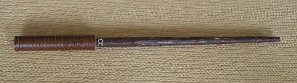
The finished Magic Wand
I try to give some information about how I have made this toy in this blog post.
I have made a movie to show the different patterns, but I noticed that the sound was not correct. This will be reuploaded at a later time.

 There is a debug interface to upload new firmware to the magic wand.

Mechanical construction

The following picture shows the main items I have used to make the magic wand: 
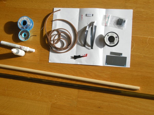
  • As base I have used a 12mm diameter wooden stick.
  • To store the electronics and batteries I have used a brass tube with an inner diameter of about the same as the outer diameter of the wood. With a bit Kapton tape is the stick stuck in the tube. This part forms the handle of the magic wand. It is also possible to use an empty tube like part such as a (whiteboard) marker.
  • A leather cord is glued to the handle to make it feel and look nice.
  • LEDs are glued with super glue to the wood before soldering the wire to each LED.  I have used 0603 for the body of the wand and 0805 for the top.  In my case I have used the colour purple for all led.
  • The electronics consist of mainly a Attiny84 with some resistors and capacitors.  
  • The chip is soldered on a piece of SMD prototype board. This has a bit of a special grid and was not perfect in that aspect but it was very thin and could be easily cut to size and fixed in the wood & tube.  I have used this.
  • The LED and electronics are connected with a 0.2mm diameter isolated copper wire. The isolation layer is burned off on the locations where I wanted to solder.
  • Paint and lacquer to colour the stick. I have used acrylic paint.
  • Furthermore is solder, flux and solder wick needed.
I have a few tips on the assembly:
  • It is difficult to get the stick in the right shape.  Clamping the stick in a drill and run it over sanding paper did not work so well.  Cutting it with plane in the right shape and sanding afterwards did work for me.  A small lathe is probably nice for this kind of round work pieces.
  • The super glue worked very well to tack the led to the wood and to solder it. A bit heat is needed to remove the glue from the led on the points where it should be soldered. But no led came of during the soldering.
  • With the solder iron on 450C is the isolation material on the copper wire quickly gone. This works better than a mechanical method (sanding paper, knife etc.) however is not good for the tip of the soldering iron.
  • I have painted clear lacquer over the LEDs after the soldering; this to protect the led and the wires. A disadvantage of this is that the light travels side ways over the magic wand. 
  • I have put first the 8 wires on the stick with tape and then put the LEDs in between and have solder them by pulling the wire to the LED.  Probably it is easier to put lines on the stick to determine the LED position, glue the led and then pull the wires from LED to led. I expect that that works better to keep things nicely oriented. 

Electrical schematic


The electrical schematic is fairly simple. PortA of the Attiny84 microcontroller is used to drive the leds.  In principle is it possible to charlieplex in this way 56 leds (N^2-N). For this design I am using only 24 leds.  The 150ohm resistors is calculated based on a 2.8V voltage drop over the led and a 5mA drive current. In the software is never more then 1 led on at the same time so this construction is from the current load on the microcontroller fairly uncritical.
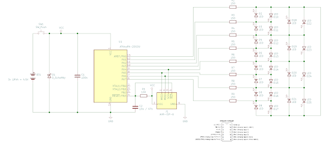
Electrical schematic of the Magic Wand
The the size of the LEDs on the body of the stick are 0603 and on the top is 0805 used.
The programming interface is working correctly when the LEDs are attached.  This does give some additional light effects when the microcontroller is programmed.
The push button is directly between the batteries and the processor board.  For testing I have used 3 AAA penlight batteries. I have used 3 stacked LR44 batteries to fit in the handle during "normal" usage.  The electrical contact points of the battery are made with thumb-tacks, which works surprisingly well.  The diode D1 protects the circuit when I forget what the + and - side of the battery should be.

With some work the electronics looks like this:
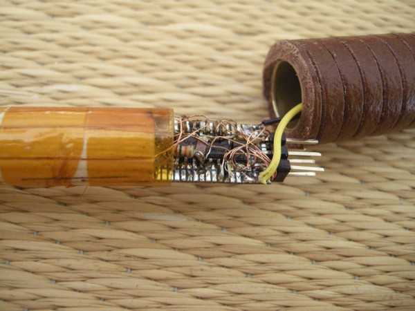
The electronics inside the magic wand.
The black wire is the (-) of the battery and the yellow the (+). The 6pin AVR ISP connector is clearly visible. The 0.2mm diameter copper wires are thin compared with the other parts.

I had to use a microscope to solder this successfully.

Software 

The firmware for the magic wand is fairly simple and written in the Arduino platform.  There is no real reason to do this; this could be done just as simple without Arduino and with a normal Makefile and avr-gcc.

A table with DDRA and PORTA values is used to address each LED correctly and to compensate for "errors" in the soldering.  By using the index in the table is each LED addressable.

The push button is connected to the power supply of the Attiny84. This means that when the button is pushed the processor gets power and comes out of the reset.  As first step is the previous animation number read out of the EEprom.
Then is the next animation shown. At the end of the animation is this new number written into the EEprom.
After this is the processor put in deep sleep to save current when the button is continuously pushed.

With this setup is it possible to repeat an animation when the button is released before the animation is finished.  A new animation    will be shown when is waited until the previous animation is finished and the push button is pushed again.

Things to improve:
  • Remove the Arduino frame work.  I am not really using it and it is probably giving some timing issues.
  • I have a flicker in the first part of each animation. Just if it is run two times.  I thought it could be because the calculations done which is adding 0 for the first ring.  But removing this with and IF statement is not solving this either.
  • Some fading or different brightness levels would be nice to add to the animations.  This must be possible with a timer interrupt but I did not had enough time before Halloween to experiment with it.
The source code:
#include <EEPROM.h>   // Items for the EEPROM
#include <avr/sleep.h>    // Sleep Modes
#include <avr/power.h>    // Power management

#define ATTINY84
#define MAXEFFECT 7
#define EEADDRESS 5

#define SLOWCYCLE 200
#define FASTCYCLE 100
#define NULLCYCLE 0

#define SLOWDELAY 400
#define FASTDELAY 200
#define NULLDELAY 3

const uint8_t dirlist[] PROGMEM  ={ B0, 
                  B00000110, B00011000, B01100000, B10000001, B00000011, B00001100, B00110000, B11000000,
                  B00000110, B00011000, B01100000, B10000001, B00000011, B00001100, B00110000, B11000000,
                  B00000101, B00010100, B01010000, B01000001, B00000101, B00010100, B01010000, B01000001 };
const  uint8_t outlist[] PROGMEM  ={ B0, 
                  B00000100, B00010000, B01000000, B00000001, B00000010, B00001000, B00100000, B10000000,
                  B00000010, B00001000, B00100000, B10000000, B00000001, B00000100, B00010000, B01000000,
                  B00000100, B00010000, B01000000, B00000001, B00000001, B00000100, B00010000, B01000000};

struct MyUseCntStruct {
   byte pattern;
   int usecnt;
};

MyUseCntStruct MyUseCnt;

void setup() {
  // put your setup code here, to run once:
   SetLed(0);
   EEPROM.get(EEADDRESS, MyUseCnt);
   MyUseCnt.pattern +=1;
   if (MyUseCnt.pattern > MAXEFFECT) MyUseCnt.pattern=0;  
}

void loop() {
  // put your main code here, to run repeatedly:
  switch (MyUseCnt.pattern) {
    case 0: 
       PatternDot();
       break;
    case 1:
       PatternRing();
       break;
    case 2:
        AllOn();
        break;
    case 3:
        TestRing();
        break;
    case 4:
        PatternLine1();
        break;
    case 5:
        PatternLine2();
        break;
    case 6:
        PatternRandom();
        break;
    case 7:
        PatternRing2();
        break;    
    default:
       PatternDot();
       break;
    }
 MyHalt();
}

void SetLed(uint8_t lednum) {
  PORTA=0; // Set all to zero before changing the led
  DDRA=pgm_read_byte_near(dirlist + lednum);
  PORTA=pgm_read_byte_near(outlist + lednum);
}

void MyHalt() {
  // function to stop the anymation and to put the processor to sleep
  SetLed(0);
  set_sleep_mode(SLEEP_MODE_PWR_DOWN);
  MyUseCnt.usecnt+=1;
  EEPROM.put(EEADDRESS, MyUseCnt);
  // now sleep
  ADCSRA = 0;            // ADC ausschalten
  power_all_disable (); 
  sleep_enable();
  sleep_cpu();             // µC schläft     
}

void RingLed(uint8_t ring, uint16_t cycle, uint16_t wait) {
  // Make a ring light
  // 0 is the ring closed to the handle and 5 is the ring at the tip.
  if (ring == 0) {
    for (uint16_t i = 0; i <= cycle; i++) {
       SetLed(1 );
       delay(wait);
       SetLed(2 );
       delay(wait);
       SetLed(3 );
       delay(wait);
       SetLed(4);
       delay(wait);
    }    
  } else {
    ring *= 4;
    for (uint16_t i = 0; i <= cycle; i++) {
       SetLed(1 + ring );
       delay(wait);
       SetLed(2 + ring );
       delay(wait);
       SetLed(3 + ring );
       delay(wait);
       SetLed(4 + ring );
       delay(wait);
    }
  }
}

void ColumLed(uint8_t column, uint16_t cycle, uint16_t wait) {
  // Make a column on the stick
  if (column ==0 ) {
      for (uint16_t i = 0; i <= cycle; i++) {
         SetLed(1);
         delay(wait);
         SetLed(5);
         delay(wait);
         SetLed(9);
         delay(wait);
         SetLed(13);
         delay(wait);
         SetLed(17);
         delay(wait);
         SetLed(21);
         delay(wait);
      }
  } else {
    for (uint16_t i = 0; i <= cycle; i++) {
       SetLed(1 + column );
       delay(wait);
       SetLed(5 + column );
       delay(wait);
       SetLed(9 + column );
       delay(wait);
       SetLed(13 + column );
       delay(wait);
       SetLed(17 + column );
       delay(wait);
       SetLed(21 + column );
       delay(wait);
    }
  }
}

void PatternDot () {
  RingLed(0,NULLCYCLE,FASTDELAY);
  RingLed(1,NULLCYCLE,FASTDELAY);
  RingLed(2,NULLCYCLE,FASTDELAY);
  RingLed(3,NULLCYCLE,FASTDELAY);
  RingLed(4,NULLCYCLE,FASTDELAY);
  RingLed(5,NULLCYCLE,FASTDELAY);
  RingLed(5,SLOWCYCLE,NULLDELAY);
}

void PatternRing() {
  RingLed(0,FASTCYCLE,NULLDELAY);
  RingLed(1,FASTCYCLE,NULLDELAY);
  RingLed(2,FASTCYCLE,NULLDELAY);
  RingLed(3,FASTCYCLE,NULLDELAY);
  RingLed(4,FASTCYCLE,NULLDELAY);
  RingLed(5,SLOWCYCLE,NULLDELAY);
}

void PatternRing2() {
  RingLed(0,FASTCYCLE,NULLDELAY);
  RingLed(1,FASTCYCLE/2,NULLDELAY);
  RingLed(2,FASTCYCLE/3,NULLDELAY);
  RingLed(3,FASTCYCLE/4,NULLDELAY);
  RingLed(4,FASTCYCLE/5,NULLDELAY);
  RingLed(5,SLOWCYCLE,NULLDELAY);
}
  
void TestRing() {
  RingLed(5, SLOWCYCLE,NULLDELAY);
}

void AllOn() {
  for (uint16_t i = 0; i <= FASTCYCLE; i++) {
    RingLed(0, NULLCYCLE,NULLDELAY);
    RingLed(1, NULLCYCLE,NULLDELAY);
    RingLed(2, NULLCYCLE,NULLDELAY);
    RingLed(3, NULLCYCLE,NULLDELAY);
    RingLed(4, NULLCYCLE,NULLDELAY);
    RingLed(5, NULLCYCLE,NULLDELAY);
  }
  RingLed(5, SLOWCYCLE,NULLDELAY);
}

void PatternLine1() {
   ColumLed(0,NULLCYCLE, FASTDELAY);
   ColumLed(1,NULLCYCLE, FASTDELAY);
   ColumLed(2,NULLCYCLE, FASTDELAY);
   ColumLed(3,NULLCYCLE, FASTDELAY);
   RingLed(5, SLOWCYCLE,NULLDELAY);
}

void PatternLine2() {
   ColumLed(0,FASTCYCLE, NULLDELAY);
   ColumLed(1,FASTCYCLE, NULLDELAY);
   ColumLed(2,FASTCYCLE, NULLDELAY);
   ColumLed(3,FASTCYCLE, NULLDELAY);
   RingLed(5, SLOWCYCLE, NULLDELAY);
}

void PatternRandom() {
    SetLed(1);
    delay(FASTDELAY/2);
    SetLed(10);
    delay(FASTDELAY/2);
    SetLed(7);
    delay(FASTDELAY/2);
    SetLed(3);
    delay(FASTDELAY/2);
    SetLed(15);
    delay(FASTDELAY/2);
    SetLed(17);
    delay(FASTDELAY/2);
    SetLed(4);
    delay(FASTDELAY/2);    
    SetLed(10);
    delay(FASTDELAY/2);    
    SetLed(2);
    delay(FASTDELAY/2);
    SetLed(18);
    delay(FASTDELAY/2);    
    SetLed(9);
    delay(FASTDELAY/2);    
    SetLed(9);
    delay(FASTDELAY/2);    
    RingLed(5, SLOWCYCLE, NULLDELAY);
}